
 2 hours ago
 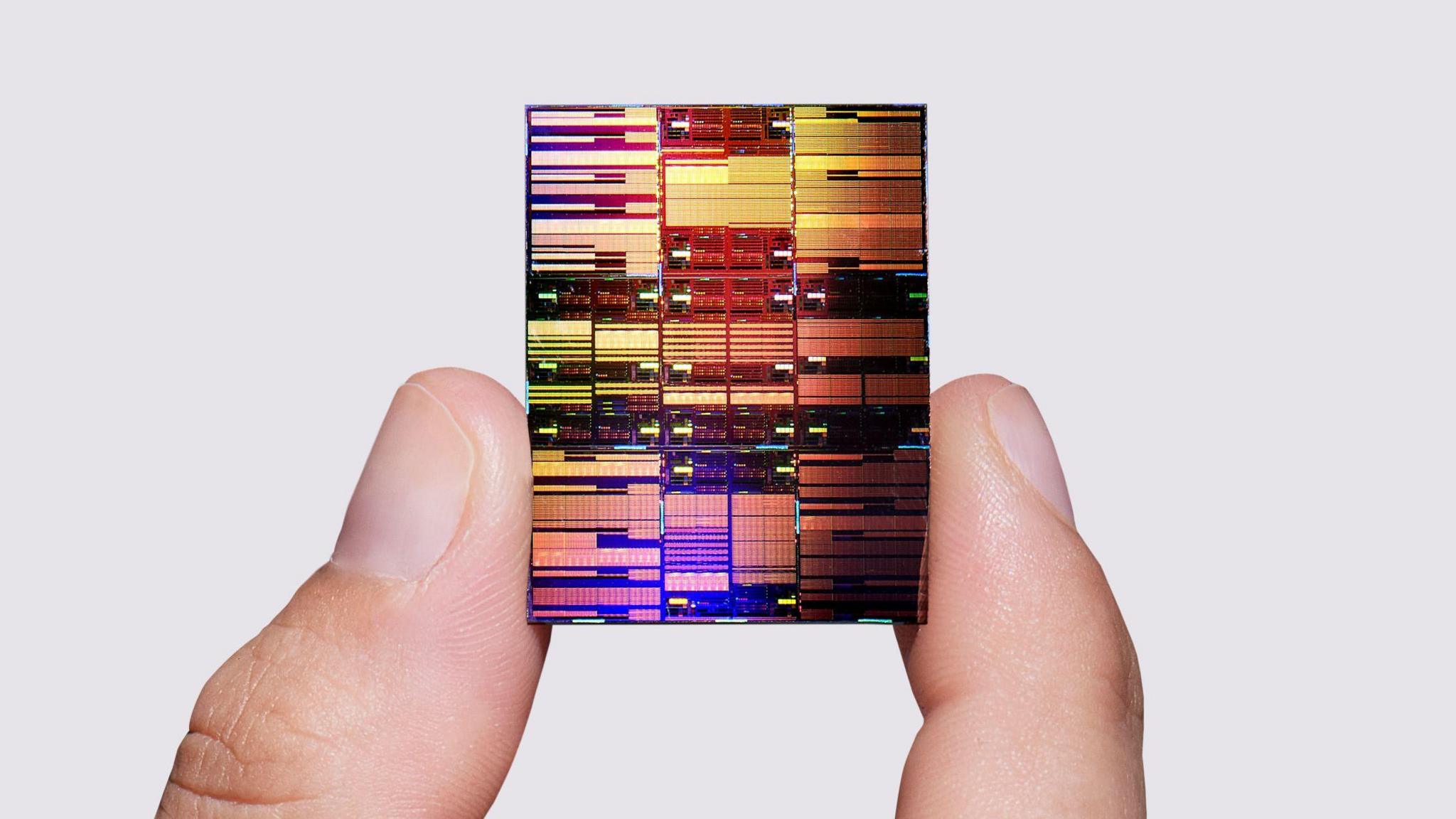 Image source, IBM
IBM's caller sub-1 nm spot crams astir 100 cardinal transistors onto a aboveground the size of a fingernail
IBM has unveiled a caller spot plan which it says could alteration manufacturers to cram 100 cardinal transistors connected a silicon spot the size of a fingernail.
The existent industry-standard size for chips, measured successful a the portion of nanometres - a billionth of a metre and the size of a fewer atoms - is astir 2 nanometres (nm).
But IBM claims its caller spot tech is the equivalent of astir 0.7nm, which whitethorn marque it the world's archetypal known spot exertion beneath 1nm.
However, it volition beryllium respective years earlier the spot tech could beryllium acceptable to spell into production.
The steadfast claims successful tests, its prototype performed 50% amended than its ain 2nm spot and was 70% much vigor efficient.
It claimed akin boosts successful show erstwhile it debuted its 2nm spot tech backmost successful 2021 - saying astatine the clip its tests of those, somewhat larger, chips produced akin leaps successful show and vigor efficiency.
Jay Gambetta, manager of IBM Research and IBM Fellow, described the NanoStack tech arsenic a "landmark moment" for the aboriginal of chips.
"With our caller NanoStack architecture, we're not conscionable making smaller transistors, we're reinventing however chips are built to present dramatically much powerfulness and vigor efficiency," helium said.
Transistors are the gathering blocks of silicon chips - which supply computing powerfulness for the world's electronics, including smartphones, games consoles and laptops.
They person besides go important to the almighty computers housed successful information centres, processing a scope of mundane integer activities from streaming to online banking, and powering the generative AI boom.
The much transistors manufacturers tin compression onto a chip, the much almighty the spot becomes, and truthful the much devices tin do.
At the aforesaid time, designers strive to marque the chips themselves ever smaller.
For decades, the fig of transistors that tin beryllium enactment onto a spot has doubled each 2 years: this is simply a improvement known arsenic Moore's Law.
But with billions of transistors present connected immoderate chips, it is increasing much hard to prolong and experts broadly hold this gait of maturation cannot proceed indefinitely.
In bid to effort to widen it, alternatively than effort to cram much transistors onto the aboveground horizontally, spot designers person for immoderate clip focused connected 3D alternatives, fundamentally altering the signifier of the transistors to marque them taller.
IBM's attack is to furniture sheets of them connected apical of each different arsenic well.
Professor Alan Woodward, a machine idiosyncratic astatine Surrey University, compared it with gathering a large artifact of flats alternatively than houses successful a city.
"IBM's NanoStack is similar proposing a 100-story skyscraper," helium said, adding that successful his view, the firm's closest rivals specified arsenic Samsung and Intel are person to 30-50 communicative buildings with their ain 3D spot work.
The challenges facing 3D spot designers see heat: the transistors tin get blistery arsenic they enactment and vigor rises.
Additionally, erstwhile the layers betwixt them are excessively thin, sometimes this prevents them from switching disconnected erstwhile they're expected to, and this stops the spot from working.
"I deliberation it's just to accidental IBM's proposals are the astir ambitious," said Prof Woodward.


 English (US)·